
As electric vehicles move toward 800-volt architectures, DC fast chargers demand more than simple circuit boards. They must manage high current, rapid switching, heat, vibration, moisture, and repeated thermal cycling. The right PCB for DC Fast Chargers can influence efficiency, service life, electromagnetic performance, and maintenance costs.
This 2026 overview examines the PCB types gaining attention across modern charging equipment. High-Tg multilayer boards support stable insulation near power modules. Heavy-copper PCBs handle demanding current paths with reduced resistance. IMS and other metal-core designs can move heat away from switching devices more effectively. HDI boards help control-board designers fit sensors, processors, communication interfaces, and protection circuits into smaller spaces.
The details matter.
A board may look suitable in a laboratory, yet fail after thousands of heating and cooling cycles. Engineers therefore examine copper thickness, dielectric selection, creepage distance, via reliability, surface finish, and connector placement. Factory process control also matters. Poor lamination or inconsistent plating can weaken an otherwise impressive design.
There is no universal winner. High-current boards may improve conduction but increase cost and manufacturing complexity. Compact HDI layouts can save space, but repairs may become less convenient. Metal-core construction can support thermal management, although it may limit routing flexibility. These trade-offs deserve honest evaluation.
Based on practical power-electronics design principles and charger reliability concerns, the following sections compare the leading PCB technologies for 2026. The goal is not to promote one material blindly, but to identify where each PCB type performs well, where it struggles, and which design choices deserve closer testing before mass production.
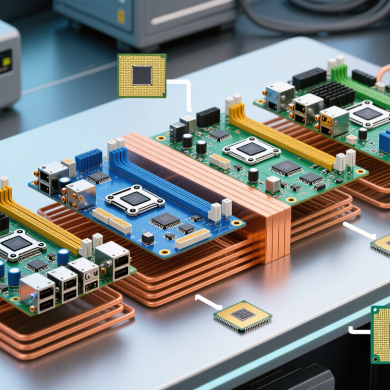
What Are the 2026 Top PCB Types for DC Fast Chargers?
DC fast chargers usually combine an AC/DC power factor correction stage, an isolated DC/DC converter, control circuits, and communication boards. Each stage creates different PCB demands. Multilayer FR-4 boards remain practical for control and monitoring circuits. Heavy-copper multilayer PCBs suit high-current paths and reduce resistive heating. Insulated metal substrate boards can improve thermal transfer near switching devices. Ceramic PCBs offer excellent heat handling, but their cost and mechanical limits require careful justification.
PCB selection should begin with the charger’s voltage, current, switching frequency, and expected duty cycle. Designers must check creepage and clearance distances, especially around high-voltage sections. Copper thickness, via structure, and connector ratings directly affect power loss. Thermal simulation helps, but physical testing still matters. Airflow, enclosure temperature, and repeated charging cycles can expose weaknesses that calculations miss. EMC performance also depends on stack-up, grounding, return paths, and component placement. A technically impressive PCB may still fail in production if it is difficult to inspect or repair.
Tips: Separate noisy power zones from sensitive control areas. Use short gate-drive loops. Add temperature sensing near hotspots. Confirm dielectric strength through qualified testing. Do not select a PCB only by its current rating; cooling conditions change the result. In practice, a balanced design is often better than the most advanced material. Some early assumptions may prove wrong, so prototype testing should remain part of the selection process.
For 2026 DC fast chargers, power PCB selection is moving beyond simple current ratings. Heavy-copper multilayer PCBs remain practical for rectifier stages, DC-DC converters, and busbar interfaces. Copper layers from 3 to 6 ounces can reduce resistance across short, high-current paths. Wide planes also spread heat from MOSFETs, diodes, and magnetic components. In production reviews, engineers should inspect via arrays, copper balance, and solder-joint stress, not only datasheet amperage. The numbers can mislead.
Insulated metal substrate PCBs suit compact power modules requiring direct thermal transfer. Aluminum-backed structures can move heat toward a cold plate, while high-Tg laminate supports repeated thermal cycling. For higher-voltage isolation, multilayer boards with controlled creepage, clearance, and reinforced insulation are more dependable. Energy-management sections may use separate control PCBs, but grounding and sensing routes must remain close to the power stage. A few millimeters of noisy routing can distort current feedback. Small details matter.
For bidirectional conversion and battery buffering, designers often combine heavy-copper outer layers with internal planes and embedded thermal vias. This arrangement supports fast switching without turning the enclosure into a furnace. Surface finishes, pad geometry, and connector anchoring also deserve laboratory validation. A prototype can pass a short load test and still fail after thousands of thermal cycles. Engineers should record hotspot temperatures, voltage drop, and insulation resistance under realistic airflow. No stackup is perfect. The right PCB balances current, heat, isolation, service life, and manufacturing tolerance.
| PCB Type | Primary DC Fast-Charger Application | Typical Copper Configuration | Typical Voltage Class | Current and Thermal Capability | Key Construction Features | Main Design Considerations |
|---|---|---|---|---|---|---|
| Heavy-Copper Multilayer PCB | AC/DC rectifier stages, high-power DC/DC converters, input and output bus distribution | 3–12 oz copper on selected power layers; lighter copper may be used for signal layers | Commonly designed for 400–1,000 V DC systems, depending on insulation and spacing design | Suitable for high-current paths from tens to several hundred amperes when copper area, vias, connectors, and cooling are properly engineered | Thick copper planes, large plated vias, parallel current paths, reinforced terminals, and controlled creepage and clearance | Higher copper weight increases etching difficulty, board thickness, thermal stress, and manufacturing cost; current sharing must be verified |
| High-Tg FR-4 Power PCB | Modular power-conversion boards, gate-driver sections, control power supplies, and charger communication assemblies | Typically 1–4 oz copper, with heavier copper added in localized power regions | Suitable for low-voltage control circuits and medium-to-high-voltage power sections when the laminate system is correctly specified | Good electrical insulation and dimensional stability; thermal performance depends strongly on copper spreading, vias, and heatsinking | High glass-transition-temperature laminate, multilayer stack-up, embedded reference planes, and reinforced plated through-holes | Requires careful dielectric selection, field control, thermal relief design, and protection against delamination during repeated thermal cycling |
| Metal-Core PCB | Power semiconductor mounting, auxiliary converters, cooling plates, and compact thermal-management assemblies | Usually 1–6 oz copper over a dielectric layer and metal base, commonly aluminum or copper | Often used in isolated or non-isolated power assemblies; working voltage depends on dielectric thickness and isolation requirements | Provides a short thermal path to a chassis or heatsink; practical current capacity is determined by copper geometry and component temperature limits | Metal heat-spreading core, thermally conductive dielectric, insulated copper circuit layer, and direct mechanical attachment to cooling hardware | Electrical isolation, coefficient-of-thermal-expansion mismatch, mounting flatness, and dielectric thermal resistance require validation |
| Insulated Metal Substrate for Power Modules | Compact switch assemblies using silicon, silicon-carbide, or gallium-nitride power devices | Thick copper circuit layer bonded to a ceramic-filled dielectric and a metal heat-spreader | Used in high-voltage switching sections when dielectric breakdown strength and creepage requirements are satisfied | Supports high power density by reducing thermal resistance between semiconductor packages and the heatsink | Low-inductance layout, closely coupled power loops, thermally conductive dielectric, and mechanically rigid baseplate | Parasitic inductance, partial discharge, thermal cycling, solder-joint fatigue, and isolation coordination are critical |
| Ceramic Power Substrate | High-frequency switching modules, high-temperature power stages, and compact converter inverter sections | Metalized copper on ceramic dielectric, commonly using direct-bonded or active-metal-brazed construction | Appropriate for high-voltage power modules when insulation thickness, edge distance, and module design meet the required rating | High thermal conductivity and low parasitic inductance support fast switching and high power density | Alumina, aluminum nitride, or other ceramic insulation with bonded copper conductors | Excellent thermal and electrical performance but higher brittleness, specialized processing, and greater cost than conventional FR-4 |
| High-Voltage Multilayer PCB | High-voltage DC bus monitoring, isolation interfaces, insulation monitoring, and energy-management control | Typically 1–3 oz copper with dedicated guard, shielding, and reference layers | Commonly designed for 400–1,000 V DC charger architectures; exact rating depends on pollution degree, material group, and spacing | Optimized for insulation reliability and signal integrity rather than maximum conductor current | Controlled creepage and clearance, slots or cutouts, conformal-coating compatibility, isolated domains, and guarded traces | Safety spacing must account for working voltage, transient overvoltage, altitude, contamination, humidity, and manufacturing tolerances |
| Low-Inductance Laminated Busbar PCB | DC-link distribution, capacitor-to-switch connections, and high-current paths between parallel power modules | Thick copper or laminated copper layers arranged as closely coupled positive and negative conductors | Frequently used in 400–1,000 V DC links, subject to insulation system and mechanical construction | Supports high pulse current while reducing loop inductance, voltage overshoot, and electromagnetic emissions | Compact conductor spacing, controlled impedance of the power loop, integrated insulation, and high-current terminal interfaces | Requires accurate mechanical tolerances, robust dielectric insulation, low-resistance joints, and careful creepage at edges and terminals |
| Rigid-Flex Power and Control PCB | Compact charger modules, moving or space-constrained assemblies, display interfaces, and auxiliary control interconnects | Usually 1–3 oz copper in rigid sections; flex sections generally use thinner copper for bend reliability | Primarily suited to control, sensing, and auxiliary power circuits rather than the highest-current DC output path | Improves packaging flexibility; current capability is limited by flex geometry, bend radius, temperature rise, and connector design | Rigid multilayer zones joined by flexible polyimide sections, strain relief, bend-limit zones, and plated transition vias | Keep high-current and high-heat components in rigid areas; control bend cycles, dynamic flexing, impedance, and thermal expansion |
| Thermally Enhanced Power-Control PCB | Gate drivers, current sensing, cooling-fan control, contactor control, protection circuits, and charger energy management | Typically 1–2 oz copper with thermal vias, copper pours, and localized heat-spreading regions | Commonly supports low-voltage control rails and isolated interfaces associated with high-voltage charger systems | Designed for stable operation across outdoor temperature ranges; thermal performance depends on component losses and enclosure airflow | Thermal-via arrays, copper heat spreaders, separated analog and power grounds, isolation barriers, and EMI filtering | Signal integrity, sensor accuracy, galvanic isolation, creepage, conducted emissions, and firmware-related safety functions must be coordinated |
Note: The values shown are representative engineering ranges for 2026 DC fast-charger designs, not universal limits. Final PCB ratings must be verified through thermal analysis, dielectric testing, creepage and clearance evaluation, short-circuit testing, and applicable charger safety requirements.
In 2026, control and communication PCBs will define how intelligently DC fast chargers operate. These boards coordinate power modules, cooling systems, payment interfaces, and vehicle data. A multilayer control PCB supports dense routing and stable signal timing. It also separates sensitive logic from high-current switching noise. Careful grounding matters.
Communication PCBs connect the charger with vehicles, backend platforms, and local networks. Designers commonly combine isolated CAN, Ethernet, and wireless interfaces. Galvanic isolation protects low-voltage circuits during faults. Shielded connectors and controlled impedance traces reduce communication errors. Short traces help.
Reliable charging requires more than fast processors. The PCB should monitor voltage, current, temperature, insulation status, and connector conditions continuously. Independent sensing paths can detect abnormal readings before they damage equipment. Secure boot and signed firmware also protect operational updates. However, security features may increase design complexity and testing time.
In field testing, heat buildup near power interfaces can surprise even experienced engineers. Our first layout was not perfect. A sensor trace crossed a noisy switching region and produced unstable readings. Re-routing it and improving the return path solved most of the issue. Some interference remained, reminding engineers to validate boards under real loads, vibration, humidity, and repeated charging cycles. Practical reliability comes from measured performance, not attractive schematics.
What Are the 2026 Top PCB Types for DC Fast Chargers?
In 2026, DC fast chargers increasingly require PCBs that manage heat, high current, and continuous duty cycles. Heavy-copper PCBs support large charging paths with lower resistance and reduced heat concentration. High-Tg FR-4 remains practical for control boards, especially when reinforced with thick copper and stronger thermal vias. Insulated metal substrate PCBs can move heat away from power components quickly. This matters near switching devices that run hot inside compact cabinets.
Safety depends on more than insulation distance. Engineers must control creepage, clearance, arc risk, and heat spreading across every layer. Ceramic PCBs offer strong insulation and stable performance in demanding power sections, but they can be less forgiving during assembly. Protective coatings may reduce moisture damage, while separated sensing circuits help limit fault propagation. Small details matter.
Reliability testing should include thermal cycling, humidity exposure, vibration, and repeated high-current operation. Field experience often reveals problems that laboratory tests miss, such as solder fatigue near heavy components or connectors loosening after months of vibration. Designers should inspect hotspot images, not only calculated temperatures. A few degrees can matter. Some teams still overbuild copper without reviewing airflow or service access. That approach seems safe, but it can increase cost and complicate repairs. The better choice depends on enclosure design, charging power, maintenance conditions, and the accuracy of the thermal model.
In 2026, DC fast chargers are moving toward PCB designs that manage heat, voltage, and compact installation better. High-Tg FR-4 remains practical for control and communication boards. It offers stable insulation and predictable processing. However, it may struggle near high-power switching sections without careful thermal planning.
Metal-core PCBs are gaining attention in power modules. Aluminum or copper bases spread heat from rectifiers and switching devices into attached heatsinks. Thick-copper layouts also support higher current paths with fewer temperature rises. Ceramic substrates provide excellent thermal performance and electrical insulation, but their brittleness and cost limit wider use. Not every charger needs them.
Field evaluations often show that thermal vias alone cannot solve hot spots. Engineers are combining copper planes, embedded busbars, short current loops, and temperature sensors. High-voltage boards also need controlled creepage and clearance distances. These details reduce insulation stress during humid outdoor operation. Rigid-flex sections can simplify connections around doors, displays, and cooling assemblies. Yet repeated bending and connector pressure still require deeper testing.
Low-loss laminates may improve high-speed communication between charging controls and monitoring circuits. Their benefits are real, but layout quality matters more than material claims. A rushed stack-up can create noise, even with premium laminate. Designers should validate prototypes across heat cycles, vibration, dust, and peak-load charging. Some early concepts remain expensive or difficult to repair. That weakness deserves more attention.
